Technologies that were considered innovative a dozen years ago have undergone significant evolution and are now found in operation in many optics manufacturing firms. Improvements in generation, finishing, assembly, and metrology technologies are being leveraged to generate higher-performing optical systems and push the upper end of the precision scale.
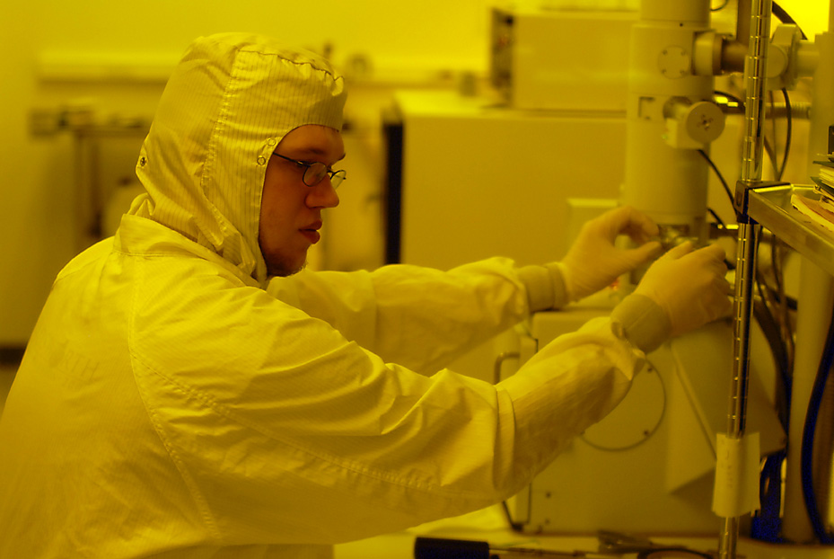
For the last several decades, photolithography has been the dominant printing technology used by integrated circuit manufacturers, and it is a key factor in increasing the transistor density per silicon area and lowering the cost per transistor.
Additive manufacturing, or 3-D printing, describes a group of technologies that are used to create parts by building up layers to, in effect, “grow a part.” Additive processes are fundamentally different from traditional subtractive processes in which material is removed from a block to create a part. One of the big advantages of additive processes is that the amount of waste material is greatly minimized because only as much source material as is needed is used to build the part.
Additive manufacturing, or 3-D printing, describes a group of technologies that are used to create parts by building up layers to, in effect, “grow a part.” Additive processes are fundamentally different from traditional subtractive processes in which material is removed from a block to create a part. One of the big advantages of additive processes is that the amount of waste material is greatly minimized because only as much source material as is needed is used to build the part.


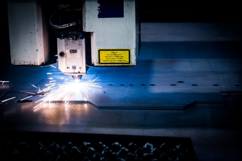
Laser systems have been transformed from tools applicable only to highly specialized processes to commonplace tools that are used extensively in shop floor operations, such as cutting, drilling, piercing, and welding. Precision lasers that are used to process materials by cutting, welding, drilling, and piercing can provide advantages over conventional processes. These include improvements in the ability to hold tight tolerances, reduction in downtime associated with setups, reduction in part cleaning and deburring, and reduction in distortion of parts during processing. Lasers not only provide the ability to cut materials but provide the ability to produce high-quality components and assemblies precisely and repeatedly.
Related Courses found in the B.S. in Photonic Science and Engineering Program at UCF:

Laser Engineering and Lab
Includes the concept of a photon, processes of interaction of light with matter (and its application to detectors), the generation of light via spontaneous and stimulated emission, atomic transitions leading to fluorescence. Properties of lasers are introduced as the basis of optical amplifiers. Optical resonators are described as a means for optical feedback. Lasers as an optical oscillator are compared to radio and microwave oscillators. Basic characteristics and types of lasers: continuous wave and pulsed lasers. Covers commercial, industrial and medical applications of lasers. Nonlinear optics and its use for wavelength conversion.

This course introduces the basic principles of two- and three-dimensional imaging systems. It includes the mathematics of image formation as a linear system and introduces point spread function, transfer function, resolution, and restoration. Objects such as microscopes, telescopes, and copiers operating in the gazing and scanning configurations are modeled and their resolution assessed. Interferometric imaging systems and their applications in metrology are described.

This class consists of analysis of optical systems consisting of lenses, mirrors, and apertures. Image plane, principal planes, and entrance and exit pupils. Magnification, field of view, F-number, image-plane irradiance. Assessment of image quality resulting from diffraction and geometrical and chromatic aberrations, using optical design software. Analysis and design of photonic systems including systems consisting of waveguides and integrated-optic components. Fidelity and noise in optical systems. Numerical simulation using photonic design software.